
1.GaN power device for fast charger market
2. GaN power device for UPS market
3. GaN power device for Electric Motorcycle market
4.GaN Power device for 5G base station market
5. GaN power device for Electric Vehicle market
6.GaN epi-wafers for HEMT market
7.GaN epi-wafers for 5G RF market
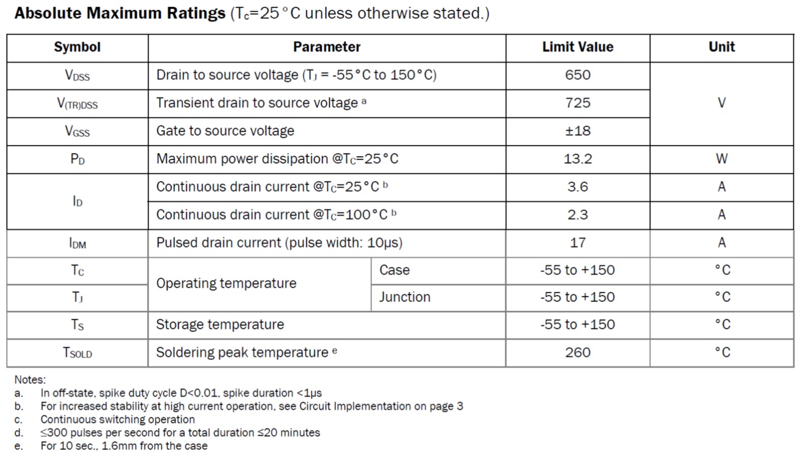
650V 480 mOhm SuperGaN GaN FET in PQFN Specs
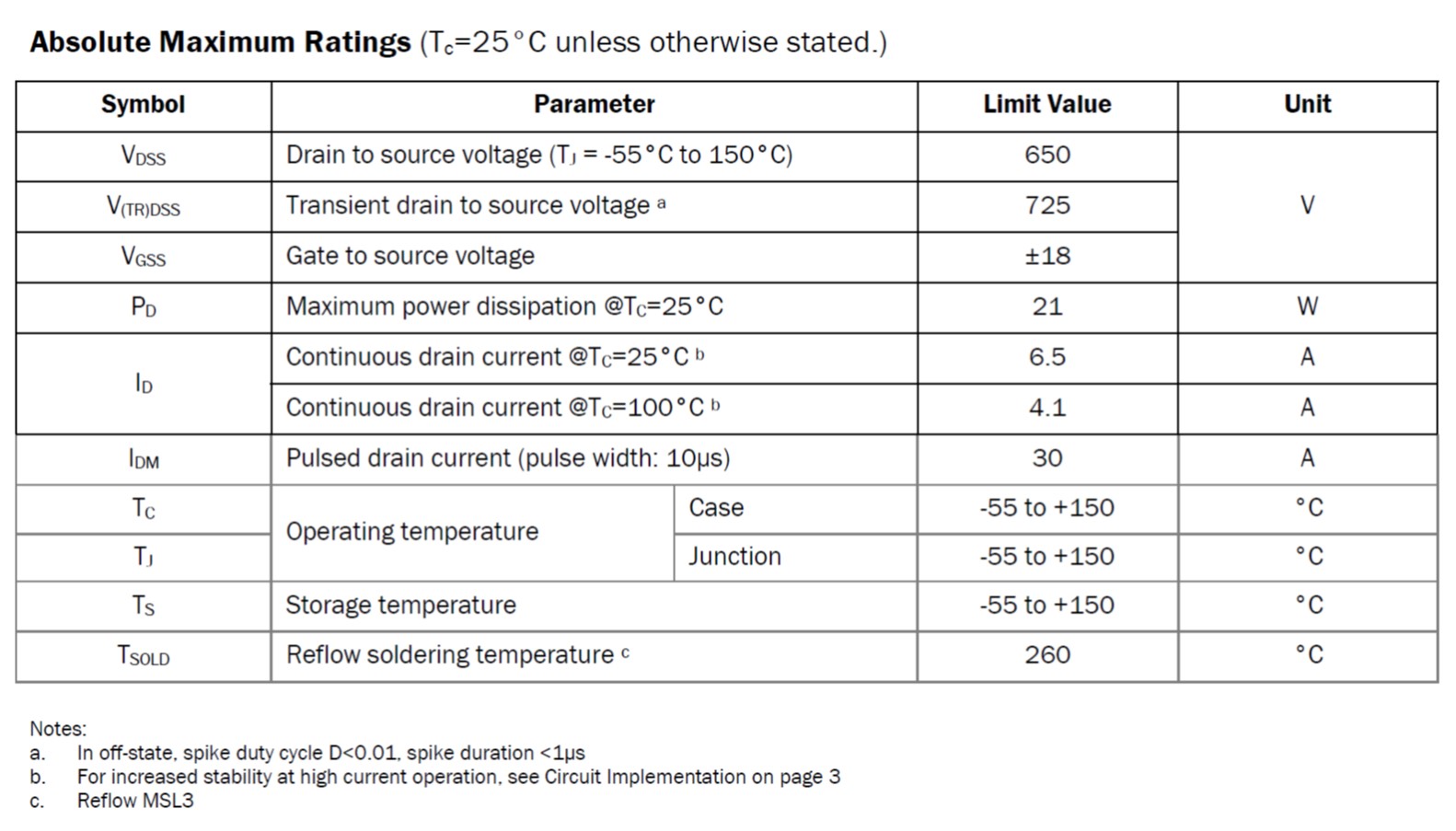
650V 240 mOhm SuperGaN™ FET in PQFN Specs
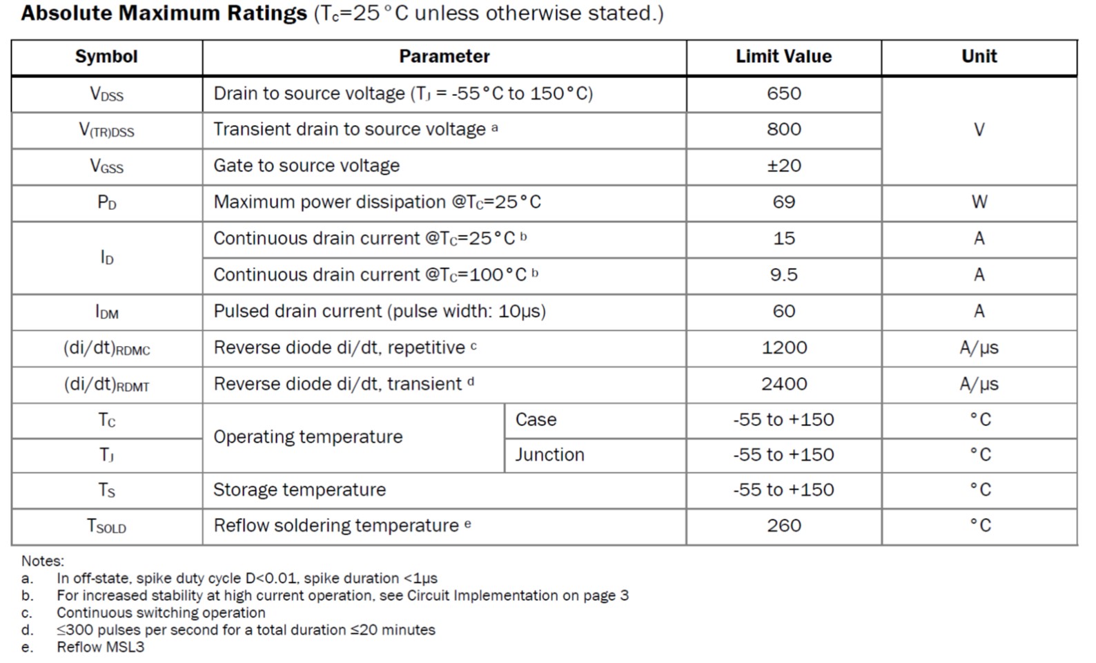
650V 150 mohm GaN FET PQFN Specs
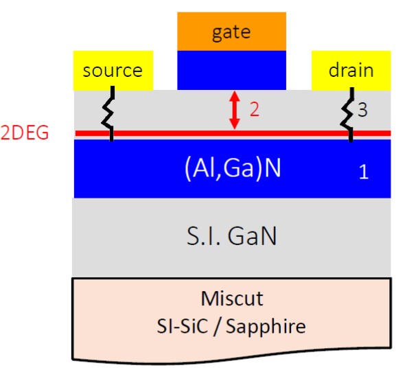
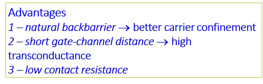
GaN Epi Wafers
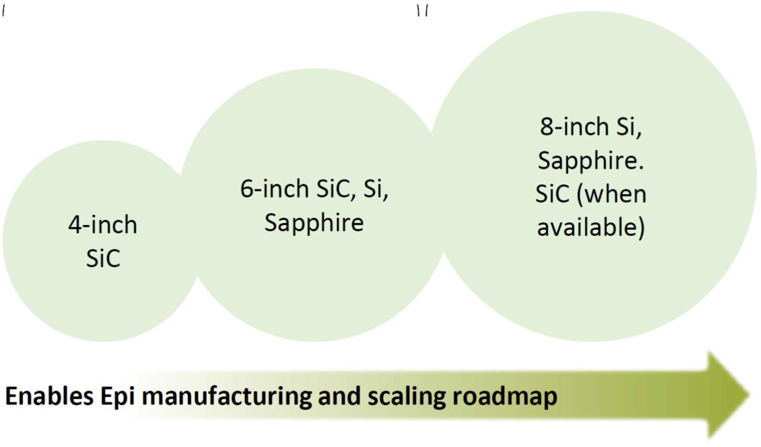
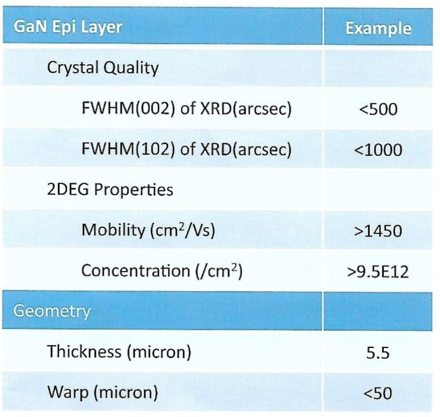
GaN Epi-Wafer Specificaitons for Power HEMT
GaN-on-SiC stands out in RF applications
1.High breakdown field: Because of GaN’s large bandgap, the GaN material has a high breakdown field, which allows the GaN device to operate at much higher voltages than other semiconductor devices. When subjected to high enough electric fields, the electrons in the semiconductor can acquire enough kinetic energy to break the chemical bond (a process called impact ionization or voltage breakdown). If impact ionization is not controlled, it can degrade the device. Because GaN devices can operate at higher voltages, they can be used in higher-power applications.
●
2.High saturation velocity: Electrons on GaN have a high saturation velocity (the velocity of electrons at very high electric fields). When combined with the large charge capability, this means that GaN devices can deliver much higher current density.The RF power output is the product of the voltage and the current swings, so a higher voltage and current density can produce higher RF power in a practically sized transistor. Simply put, GaN devices can produce much higher power density.
●
3.Outstanding thermal properties: GaN-on-SiC devices exhibit outstanding thermal properties, due largely to the high thermal conductivity of SiC. In practical terms, this means that GaN-on-SiC devices don’t get as hot as GaAs or Si devices when dissipating the same power. A “colder” device means a more reliable device.